



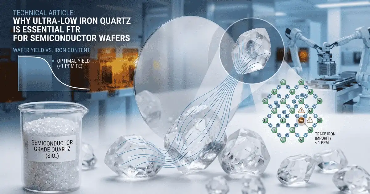
For a single lot of 300mm silicon wafers, the accumulated processing cost can reach hundreds of thousands of dollars by the time they reach electrical test. Sometimes, the problem isn't a lithography tool or an etch recipe, but a raw-material choice made months ago: the purity of the quartz material in the vessel where the melt was fused. Iron contamination at the point of crystal growth doesn't show up until wafers reach electrical test. By then, the failure has been amplified through all the depositions, implants, metrology, etc., between crystal growth and electrical test.
To process engineers and procurement staff looking to purchase silicon wafer raw materials, the purity requirement specified on a bag of quartz sand isn't a mere formality. It directly affects device yield, reliability, and long-term field performance, and it can be traced back to the material. That's why quartz sand with ultra-low iron content is a special category, completely different from quartz sand used in other sectors of the glass, foundry, and photovoltaic industry.
After all, semiconductor manufacturing is a contamination control job. Devices are composed of structures at the nanometer scale, and the electrical properties of a transistor or memory cell depend on dopant concentrations with extraordinary precision. Add an unwanted metal species, foremost iron, anywhere upstream of that framework, and you’ll see:
These failure modes typically don't become apparent until a significant number of downstream process steps have occurred, and the further downstream they are detected, the more expensive the contamination becomes. A raw material issue that might have been avoided when obtaining the sand results in a scrapped boule, a failure in the reliability test, and/or, at best, a return to the field. The economic reason for low-Fe2O3 silica sand is earlier purity control, which lowers the cost of avoiding the defect.
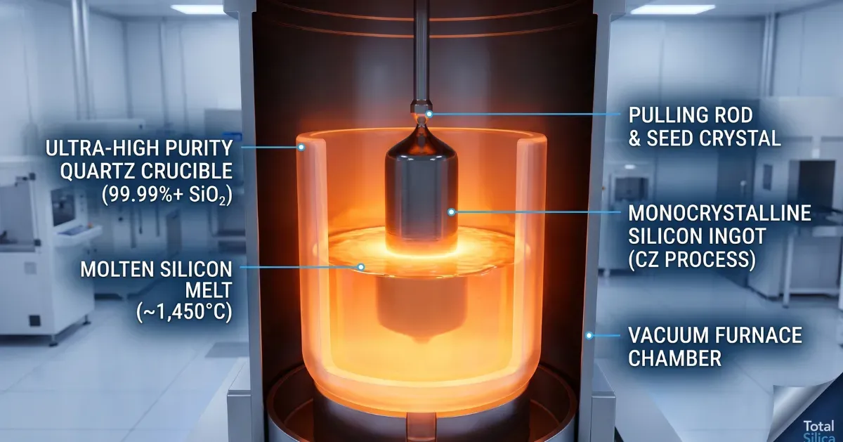
Tracing the sand's path helps explain why high purity matters when the wafer is finished. Of the silicon that is used for making semiconductors, the overwhelming majority is grown by the Czochralski (CZ) process, in which a single dislocation-free crystal is removed from a melt of polysilicon in a fused quartz crucible at a temperature of approximately 1,420–1,450°C, as it is slowly withdrawn and rotated.
These quartz crucibles are made by melting a very high-purity sample of quartz sand grains in an electric arc or plasma furnace to form a continuous shell of fused silica. That crucible is in direct and prolonged contact with molten silicon for hours or days per pull. No matter how pure the quartz starting material for the polysilicon is, there is enough time and heat to allow any iron in the starting material to diffuse to the interface and into the melt.
Most procurement specifications overlook the fact that, no matter how perfect the polysilicon is, if the crucible wall itself is the source of contamination, the ingot will be contaminated. A second, independent risk is a furnace fused from lower-purity sand, which has poor thermal shock resistance. As the furnace ramps up to the desired temperature, the crucibles must reach and maintain that temperature without cracking, spalling, or significant devitrification of the inner wall throughout the entire pull, which may last several days. If impurities cause devitrification (crystallization of the quartz's amorphous surface), the surface can flake into the melt, introducing particulate defects in addition to metallic impurities that can dissolve.
This is why both fabs and crucible fabricators deal only with a high-purity quartz sand supplier specially formulated for high-temperature fusion, rather than a generic industrial supplier. The sand's chemistry must be controlled in both its composition and its behavior under sustained thermal loading.
For the most part, the trace element impurities monitored for high-purity silica specifications are the common elements found in natural quartz stones, and the one that is most closely monitored is Fe₂O₃ (iron (III) oxide) for good reason: iron is a common contaminant in quartz and also very detrimental to the electrical properties of silicon when present in very low concentrations.
The equilibrium segregation coefficient of iron in molten silicon is very low (8 × 10⁻6), implying that iron will be strongly rejected by the solidifying lattice and returned to the melt. In principle, the CZ process has a natural partial self-purifying effect. In reality, it poses a new problem: the iron concentration in the remaining melt continues to increase as the pull progresses, increasing contamination toward the end of the ingot and reducing the ingot length for each boule from the undersized crucible.
Iron introduced or diffused into the high-temperature process will not remain in solution. It forms iron silicide at lattice discontinuities (such as dislocations, grain boundaries). These precipitates are electrically active, and that's where the failure modes that the procurement and process teams care about come from:
These failure modes are not theoretical; they are the typical categories process engineers use to trace yield excursions when correlating them with an ingot, crucible lot, or raw material batch.
There is no uniformity in the manufacture of quartz sand, and the differences in grades are much greater than the percentage value indicates. The comparison below illustrates the difference between the materials used for semiconductors and those used in glass or foundry applications; when evaluating silica sand for use in a semiconductor, purity (SiO₂) of 99.99% / 4N grade and low ppm iron content is a completely different category that is not found in foundry or glass applications.
|
Grade |
SiO₂ Purity |
Iron (Fe₂O₃) Content |
|
Standard Industrial Silica |
98.5%–99.0% |
< 150–300 PPM |
|
Solar-Grade Quartz Sand |
99.5%–99.8% |
< 50–90 PPM |
|
Electronic/Semiconductor Grade |
99.99%+ (4N Grade) |
< 1–5 PPM |
The transition from solar-grade to true semiconductor silica sand reduces the allowable iron content by up to a factor of 90. This difference exists because PV-grade performance can degrade due to carrier lifetime and defect concentration levels that would make it unusable for logic or memory. Even if the apparent SiO₂ percentage is close to high-tech, it is not solar-grade and cannot be used in semiconductors.
At the top of this hierarchy, electronic-grade quartz sand, sometimes called either 4N grade or 4N purity, is not only measured in parts-per-million (ppm) but is also now routinely measured in parts-per-billion (ppb) for the most demanding crucible-grade applications, where even single-digit ppm Fe is treated as a coarse upper bound rather than a target.
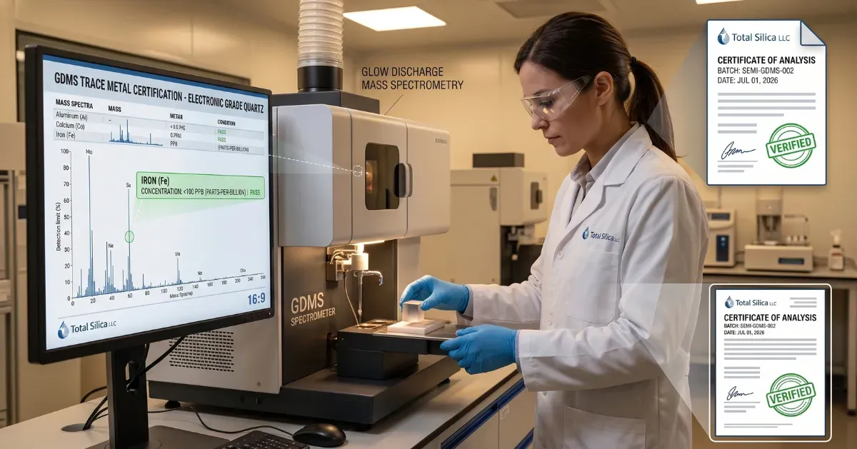
A declared specification is only as valid as the testing behind it. In practice, the procurement pain point that matters most is: "A lab report that can't be independently trusted is worse than no lab report at all," because the material hasn't been verified to spec.
Two analytical methods support credible trace element verification for high-purity silica:
Although it is usually used alongside these two methods, XRF spectroscopy is also rapid and non-destructive. It is well suited for incoming material screening at the point of receipt, even though its typical detection limits are coarser than those of ICP-OES or GDMS for ppm/ppb-level certification work.
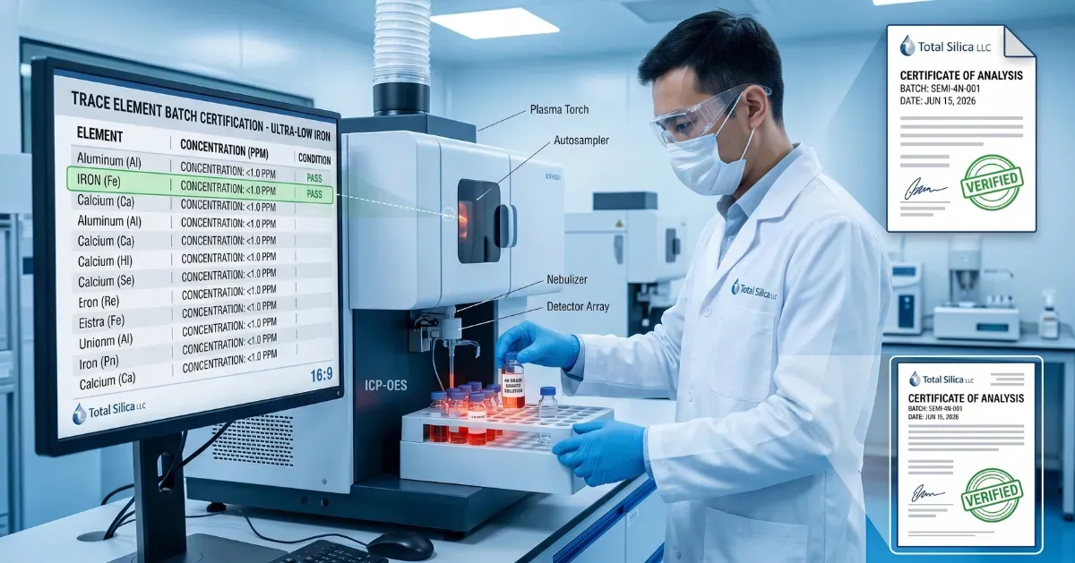
A Certificate of Analysis (COA) must always be provided and must include the actual test results (not just nominal specification claims), along with a date and a traceable batch number. When requesting a Certificate of Analysis (COA) for a specific shipment of quartz sand before using it in crucible manufacturing or directly in the process, the procurement and quality teams should not rely on a general product data sheet. The difference between the two lies in the fact that one is a marketing claim and the other a verified result.
A supplier, even if it meets electronic-grade specifications on a good day, still poses a risk if its performance isn't consistent from one lot to the next, since natural quartz deposits vary geologically. Iron content can vary between shipments even when the supplier's stated specification remains the same on paper, in the absence of close control over both sourcing and beneficiation.
For procurement managers, the practical mitigations are simple but non-negotiable:
Manufacturing high-purity quartz sand that ensures each consignment has consistent, independently verified purity eliminates one of the major variables in an already highly variable process.
The Fe₂O₃ content in electronic/semiconductor-grade quartz sand (4N, 99.99%+ SiO₂) must be below 1–5 PPM, which is a much more stringent requirement than that for solar-grade material (50–90 PPM) or ordinary industrial silica (150–300 PPM). In applications involving crucible fabrication, many specifications treat single-digit ppm as a maximum limit rather than a target, and GDMS testing is used to verify results at ppb-level resolution.
Since iron has a very low segregation coefficient, most of it is rejected into the melt rather than being taken up into the solid lattice; however, any iron that does get incorporated, or that diffuses in from a contaminated crucible wall as a result of the high-temperature processing, precipitates in the form of iron silicide at dislocations and grain boundaries, and these precipitates function as recombination centers which reduce the lifetime of the minority carriers, cause stacking faults to nucleate as a result of oxidation, and disturb the dislocation-free lattice structure which the Czochralski process is intended to produce.
ICP-OES (Inductively Coupled Plasma Optical Emission Spectroscopy) is the standard method for rapid, routine quality control to detect ppm-level impurities. For more rigorous certification, especially for parts-per-billion (ppb) resolution required in crucible fabrication, GDMS (Glow Discharge Mass Spectrometry) is the preferred analytical technique.
The problem of trace iron contamination stems from the raw materials and can therefore be solved by addressing them. Total Silica selects and tests electronic-grade silica sand for use in fabricating CZ crucibles and other high-purity semiconductor applications, and each batch is verified by an independent laboratory.
More spec sheets state that it's high purity than actually prove it. You'll find ten different pu
READ FULLFor a single lot of 300mm silicon wafers, the accumulated processing cost can reach hundreds of t
READ FULLSilica sand is widely present in modern industries. It is used in glass, construction, oil and ga
READ FULL